- 您现在的位置:买卖IC网 > Sheet目录1992 > DAC8562FP (Analog Devices Inc)IC DAC 12BIT PARALLEL 5V 20-DIP
DAC8562
REV. A
–5–
OPERATION
The DAC8562 is a complete ready to use 12-bit digital-to-
analog converter. Only one +5 V power supply is necessary for
operation. It contains a voltage-switched, 12-bit, laser-trimmed
digital-to-analog converter, a curvature-corrected bandgap refer-
ence, a rail-to-rail output op amp, and a DAC register. The par-
allel data interface consists of 12 data bits, DB0–DB11, and a
active low CE strobe. In addition, an asynchronous CLR pin
will set all DAC register bits to zero causing the VOUT to be-
come zero volts. This function is useful for power on reset or
system failure recovery to a known state.
D/A CONVERTER SECTION
The internal DAC is a 12-bit voltage-mode device with an out-
put that swings from AGND potential to the 2.5 volt internal
bandgap voltage. It uses a laser trimmed R-2R ladder which is
switched by N channel MOSFETs. The output voltage of the
DAC has a constant resistance independent of digital input
code. The DAC output (not available to the user) is internally
connected to the rail-to-rail output op amp.
AMPLIFIER SECTION
The internal DAC’s output is buffered by a low power con-
sumption precision amplifier. This low power amplifier contains
a differential PNP pair input stage which provides low offset
voltage and low noise, as well as the ability to amplify the zero-
scale DAC output voltages. The rail-to-rail amplifier is config-
ured in a gain of 1.6384 (= 4.095 V/2.5 V) in order to set the
4.095 volt full-scale output (1 mV/LSB). See Figure 3 for an
equivalent circuit schematic of the analog section.
R1
R2
VOUT
RAIL-TO-RAIL
OUTPUT
AMPLIFIER
R
BANDGAP
REFERENCE
REFOUT
2.5V
2R
R
2R
SPDT
N ch FET
SWITCHES
2R
AV = 4.096/2.5
= 1.636V/V
VOLTAGE SWITCHED 12-BIT
R-2R D/A CONVERTER
BUFFER
Figure 3. Equivalent DAC8562 Schematic of
Analog Portion
The op amp has a 16
s typical settling time to 0.01%. There
are slight differences in settling time for negative slewing signals
versus positive. See the oscilloscope photos in the Typical Per-
formances section of this data sheet.
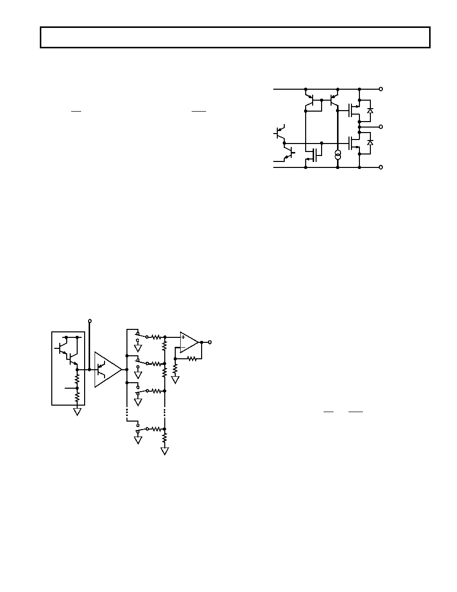
OUTPUT SECTION
The rail-to-rail output stage of this amplifier has been designed
to provide precision performance while operating near either
power supply. Figure 4 shows an equivalent output schematic of
the rail-to-rail amplifier with its N channel pull down FETs that
will pull an output load directly to GND. The output sourcing
current is provided by a P channel pull-up device that can sup-
ply GND terminated loads, especially important at the –5%
supply tolerance value of 4.75 volts.
VDD
VOUT
AGND
N-CH
P-CH
Figure 4. Equivalent Analog Output Circuit
Figures 5 and 6 in the typical performance characteristics sec-
tion provide information on output swing performance near
ground and full scale as a function of load. In addition to resis-
tive load driving capability, the amplifier has also been carefully
designed and characterized for up to 500 pF capacitive load
driving capability.
REFERENCE SECTION
The internal 2.5 V curvature-corrected bandgap voltage refer-
ence is laser trimmed for both initial accuracy and low tempera-
ture coefficient. The voltage generated by the reference is
available at the REFOUT pin. Since REFOUT is not intended
to drive external loads, it must be buffered–refer to the applica-
tions section for more information. The equivalent emitter fol-
lower output circuit of the REFOUT pin is shown in Figure 3.
Bypassing the REFOUT pin is not required for proper opera-
tion. Figure 7 shows broadband noise performance.
POWER SUPPLY
The very low power consumption of the DAC8562 is a direct
result of a circuit design optimizing use of the CBCMOS pro-
cess. By using the low power characteristics of the CMOS for
the logic, and the low noise, tight matching of the complemen-
tary bipolar transistors, good analog accuracy is achieved.
For power-consumption sensitive applications it is important to
note that the internal power consumption of the DAC8562 is
strongly dependent on the actual logic-input voltage-levels
present on the DB0–DB11, CE and CLR pins. Since these in-
puts are standard CMOS logic structures, they contribute static
power dissipation dependent on the actual driving logic VOH and
VOL voltage levels. The graph in Figure 9 shows the effect on to-
tal DAC8562 supply current as a function of the actual value of
input logic voltage. Consequently for optimum dissipation use
of CMOS logic versus TTL provides minimal dissipation in the
static state. A VINL = 0 V on the DB0–DB11 pins provides the
lowest standby dissipation of 600
A with a +5 V power supply.
发布紧急采购,3分钟左右您将得到回复。
相关PDF资料
DS1004Z-5+T
IC DELAY LINE 5TAP 25NS 8-SOIC
DS1005-125+
IC DELAY LINE 5TAP 125NS 14-DIP
DS1007S-2+T&R
IC DELAY LINE 4NS 16-SOIC
DS1010S-50+T&R
IC DELAY LINE 10TAP 16-SOIC
DS1013S-25+T&R
IC DELAY LINE 25NS 16-SOIC
DS1020S-50+T
IC DELAY LINE 256TAP 16-SOIC
DS1021S-50+T&R
IC DELAY LINE 256TAP 16-SOIC
DS1023S-25+W
IC DELAY LINE 256TAP 16-SOIC
相关代理商/技术参数
DAC8562FPZ
功能描述:IC DAC 12BIT PARALLEL 5V 20-DIP RoHS:是 类别:集成电路 (IC) >> 数据采集 - 数模转换器 系列:- 产品培训模块:Lead (SnPb) Finish for COTS
Obsolescence Mitigation Program 标准包装:50 系列:- 设置时间:4µs 位数:12 数据接口:串行 转换器数目:2 电压电源:单电源 功率耗散(最大):- 工作温度:-40°C ~ 85°C 安装类型:表面贴装 封装/外壳:8-TSSOP,8-MSOP(0.118",3.00mm 宽) 供应商设备封装:8-uMAX 包装:管件 输出数目和类型:2 电压,单极 采样率(每秒):* 产品目录页面:1398 (CN2011-ZH PDF)
DAC8562FR
制造商:未知厂家 制造商全称:未知厂家 功能描述:12-Bit Digital-to-Analog Converter
DAC8562FRU
功能描述:IC DAC 12BIT PARALLEL 5V 20TSSOP RoHS:否 类别:集成电路 (IC) >> 数据采集 - 数模转换器 系列:- 产品培训模块:Data Converter Fundamentals
DAC Architectures 标准包装:750 系列:- 设置时间:7µs 位数:16 数据接口:并联 转换器数目:1 电压电源:双 ± 功率耗散(最大):100mW 工作温度:0°C ~ 70°C 安装类型:表面贴装 封装/外壳:28-LCC(J 形引线) 供应商设备封装:28-PLCC(11.51x11.51) 包装:带卷 (TR) 输出数目和类型:1 电压,单极;1 电压,双极 采样率(每秒):143k
DAC8562FRU-REEL7
功能描述:IC DAC 12BIT PARALLEL 5V 20TSSOP RoHS:否 类别:集成电路 (IC) >> 数据采集 - 数模转换器 系列:- 产品培训模块:Data Converter Fundamentals
DAC Architectures 标准包装:750 系列:- 设置时间:7µs 位数:16 数据接口:并联 转换器数目:1 电压电源:双 ± 功率耗散(最大):100mW 工作温度:0°C ~ 70°C 安装类型:表面贴装 封装/外壳:28-LCC(J 形引线) 供应商设备封装:28-PLCC(11.51x11.51) 包装:带卷 (TR) 输出数目和类型:1 电压,单极;1 电压,双极 采样率(每秒):143k
DAC8562FRUZ
功能描述:IC DAC 12BIT PARALLEL 5V 20TSSOP RoHS:是 类别:集成电路 (IC) >> 数据采集 - 数模转换器 系列:- 产品培训模块:Data Converter Fundamentals
DAC Architectures 标准包装:750 系列:- 设置时间:7µs 位数:16 数据接口:并联 转换器数目:1 电压电源:双 ± 功率耗散(最大):100mW 工作温度:0°C ~ 70°C 安装类型:表面贴装 封装/外壳:28-LCC(J 形引线) 供应商设备封装:28-PLCC(11.51x11.51) 包装:带卷 (TR) 输出数目和类型:1 电压,单极;1 电压,双极 采样率(每秒):143k
DAC8562FS
功能描述:IC DAC 12BIT PARALLEL 5V 20-SOIC RoHS:否 类别:集成电路 (IC) >> 数据采集 - 数模转换器 系列:- 产品培训模块:Data Converter Fundamentals
DAC Architectures 标准包装:750 系列:- 设置时间:7µs 位数:16 数据接口:并联 转换器数目:1 电压电源:双 ± 功率耗散(最大):100mW 工作温度:0°C ~ 70°C 安装类型:表面贴装 封装/外壳:28-LCC(J 形引线) 供应商设备封装:28-PLCC(11.51x11.51) 包装:带卷 (TR) 输出数目和类型:1 电压,单极;1 电压,双极 采样率(每秒):143k
DAC8562FS-REEL
功能描述:IC DAC 12BIT PARALLEL 5V 20-SOIC RoHS:否 类别:集成电路 (IC) >> 数据采集 - 数模转换器 系列:- 产品培训模块:Data Converter Fundamentals
DAC Architectures 标准包装:750 系列:- 设置时间:7µs 位数:16 数据接口:并联 转换器数目:1 电压电源:双 ± 功率耗散(最大):100mW 工作温度:0°C ~ 70°C 安装类型:表面贴装 封装/外壳:28-LCC(J 形引线) 供应商设备封装:28-PLCC(11.51x11.51) 包装:带卷 (TR) 输出数目和类型:1 电压,单极;1 电压,双极 采样率(每秒):143k
DAC8562FSZ
功能描述:IC DAC 12BIT PARALLEL 5V 20SOIC RoHS:是 类别:集成电路 (IC) >> 数据采集 - 数模转换器 系列:- 标准包装:1 系列:- 设置时间:4.5µs 位数:12 数据接口:串行,SPI? 转换器数目:1 电压电源:单电源 功率耗散(最大):- 工作温度:-40°C ~ 125°C 安装类型:表面贴装 封装/外壳:8-SOIC(0.154",3.90mm 宽) 供应商设备封装:8-SOICN 包装:剪切带 (CT) 输出数目和类型:1 电压,单极;1 电压,双极 采样率(每秒):* 其它名称:MCP4921T-E/SNCTMCP4921T-E/SNRCTMCP4921T-E/SNRCT-ND